If you’ve been building circuits for any length of time, you probably know you need decoupling capacitors to keep your circuits stable. But even though it’s a favorite technique of ours, just scattering some around your PCB and hoping for the best isn’t necessarily the best approach. If you want to dig deeper into the why and how of decoupling, check out [Stephen Fleeman’s] post on the topic.
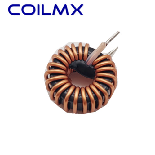
It is easy to think of capacitors as open circuits at DC and short circuits at high frequencies, shunting noise to ground. But the truth is more complex than that. Stray resistance and inductance mean that your simple decoupling capacitor will have a resonant frequency. This limits the high frequency protection so you often see multiple values used in parallel to respond to different frequencies. Inductance In Parallel
Because the stray resistance and inductance plays a part, you may want to use fatter traces — less resistance — and shorter runs for less inductance. Of course, you can also use power and ground planes on the PCB as a form of decoupling. At the end of the post, [Stephen] talks a little about the importance of digital and analog ground that interact in a specific way.
If you want to do some empirical testing, you can build a test rig and do the work. Or check with [Bil Herd] about PCB inductance.
Somehow I expected the link to be a youtube video I could watch, zone out and not learn much from.
NO, PLEASE, NO! If you want to prevent engineers to make the same mistakes again and again, then, please delete this hackaday post or, at least, delete the link to [Stephen Fleeman’s] post on the topic.
It is exactly the way you DON’T DO IT.
If you want to learn from real experts then, PLEASE, go and see or read some videos/books from Eric Bogatin, Todd Hubing, Henry Ott, Steven Sandler, Rick Hartley, …
Eric Harris also has a nice video about capacitors.
Please provide a specific article, not just vague references to a huge list of possible videos or books.
The answer is that there is no specific article, because there is no quick and easy answer.
Power design and proper decoupling doesn’t have a “one size fits all” answer. Learn how to simulate it with real component behavior (including inrush current at startup!) and parasitics and then measure it and tweak.
For simple situations, this article’s massive overkill – a single 0.1 uF cap as small as you’re comfortable using near each power pin will handle things. For more complicated ones, it’s nowhere near good enough.
Take these references as an entry point:
– https://www.youtube.com/watch?v=ySuUZEjARPY&ab_channel=Altium – https://www.youtube.com/watch?v=vALt6Sd9vlY&ab_channel=RobertFeranec – https://www.youtube.com/watch?v =y4REmZlE7Jg&ab_channel=AltiumAcademy – https://www.youtube.com/watch?v=DIMIzKRmync&ab_channel=Altium – https://www.amazon.com/-/de/dp/013451341X – https://www.amazon.com /-/de/dp/0470189304 – https://www.amazon.com/-/de/dp/0071830995
Once you got on the “right” track you will spot the good from the bad literature/videos quite fast. As far as I know most of the myths (separate ground planes, paralleled capacitors, …) stems from low quality application notes of semiconductor manufacturers. And yes, MS-BOSS is quite right, I am somewhat angry because there are so many good resources and it has never been easier to reach them (for free). So again my advise, please delete the link to this blog post.
I read the article “The Myth of Three Capacitor Values” from Eric Bogatin. He doesn’t really disagree with the article from this HaD post. Rather he says that for very advanced manufacturing techniques is outdated, and mostly applies to THT. For surface mount you don’t need 3 capacitors, since MLCC caps (surface mount ones) will have the same inductance, no matter their capacitance (as they are usually available in the same physical size, not like THT caps).
The HaD linked article is a bit vague, but otherwise seems reasonable, that would apply to most projects with a 2 layer board and some THT components.
What matters is to also add the new design rules to your arsenal as mentioned in some of the linked articles here, but the old ones are not wrong, they just apply to, frankly for the hobbyist, for common build scenarios (THT, or two layer surface mount, except for the 3 cap rule, as mentioned above).
But yes, it is very vague.
There’s… not really any recommendations in the HaD linked article I agree with from a PDN point other than “use planes” – and even that’s more subtle than is outlined.
The “electrolytic handles low-frequency” is too vague to even be useful: large (“bulk”) capacitors don’t need to be electrolytic, you don’t need one per IC, and they interact more with the supply regulation anyway. You might not even need them if the regulator’s got a fast enough transient response (outside of what the regulator needs, obviously). Electrolytics can help damp resonances, but only if they’ve got a high ESR, and not all of them do anymore.
If you need decoupling past resonance, multiple caps in parallel won’t help. You need a lower-inductance cap.
Throwing ferrite beads like is done in that example can be extremely dangerous: http://iconnect007.com/index.php/article/123867/quiet-power-do-you-really-need-that-ferrite-bead-in-the-pdn/123870/ That’s just one problem as well: consider what happens when there’s a load transient behind a ferrite bead – the voltage drop at the load will be significantly worse, possibly enough to cause the circuit to fail. There are plenty of good uses for ferrites, you just have to know what you’re trying to do.
Blindly splitting grounds is terrible. Putting ground plane *voids* can work to keep stray low-frequency currents out of a sensitive section. But there’s zero reason for a “tie at a single point” rule. https://www.edn.com/partitioning-and-layout-of-a-mixed-signal-pcb-2/ http://www.cn-william.com/uploadfile/documents/e2v/application%20note/Board-Layout.pdf
And even that second example PDF isn’t great. You’re not necessarily trying to isolate *components*, you’re trying to isolate *return currents*. So you need to consider everything when partitioning, including power.
It’s just… not good.
The reason why Hans got so angry is (I assume) the fact that once any of the inductors gets inductive, it IS INDUCTIVE. And what happens when you place an inductor in parallel to a capacitor? Oh yes, it resonates. And if you have several capacitors in parallel and one goes into resonance at a few MHz, then likely the whole bank will resonate (not necessarily at that frequency, but it will somewhere). So instead of making it better, you’re only making it worse probably. The electrolytic cap may dampen the network using its ESR, but it may not be enough.
Also, it is wise to remember that simple RLC models of capacitors rarely fit actual measured performance very well, more complicated models are needed often.
Also the supposed layer change instead of same-layer trace is often wrong. The inductance and electrical length of the via may make it much worse – we found that on BGAs with caps on bottom side. It was better to route them to the side on top layer.
Another thing with the separate grounds – where and how do they connect? What if they’re connected 20 cm away. Is that low impedance connection enough? What if some noise is injected in it? All of the circuits along the way may be affected by it.
TL;DR: the article is bad. As if written by a non-engineer, but a theoretic.
“The electrolytic cap may dampen the network using its ESR, but it may not be enough.”
Yeah, it’s really worth noting that although we tend to think of “low ESR” as being “good” for a capacitor, it can often be very, very bad. Very low ESR caps in a power distribution network can cause a large initial overshoot when the supply first turns on if the supply’s got a very low output impedance, which can eventually destroy caps which are sometimes only slightly derated (e.g. a 6.3V cap on a 5V rail).
Which is why you can’t really come up with “general rules” for this stuff. I can come up with a decoupling/bypass network which works perfectly fine when handled by a supply with a proper soft-start, but then you move it over to a different application where the supply just turns on immediately and the whole thing fails.
You can easily loose track of what the original goal is in all this. You’re trying to keep the +5V (or whatever voltage you are using) from developing noise on the power. This can feed to other chips causing them to hiccup. The best way I have found to do this is put the cap as close physically to the chip it is protecting as possible. This suppresses any inductance that might form from the traces leading up to the part. Commonly the bypass cap is placed under the chil on the other side of the PCB. This makes the traces very short, and hence little parasitic inductance. You can’t eliminate the resonance, but you can push it outside of the frequency range that maters to your circuit.
The “noise” on the power comes from transient current draws from each of the loads on the supply. How much that current draw translates into voltage changes on the supply seen by that chip (and the others) depends on a *ton* of things – very much so including the supply itself. You can need very different decoupling networks with the exact same loads if they’re powered by different supplies.
The key is to understand at what level you need to keep things at. It also doesn’t hurt to give yourself options in the early stages: multiple footprints for optional parts, for instance, or at least a test point where you can supply power directly.
“Commonly the bypass cap is placed under the chil on the other side of the PCB. This makes the traces very short”
I disagree: *if at all possible* the bypass cap should be on the same side as the chip it’s bypassing. Unless it’s a BGA (and often times even then) you can usually put a bypass cap closer to the supply pin than 1.6 mm: remember, the traces *include* the via length.
Exactly right. Lower ESR = high Q, and high Q can be a recipe for really nasty ringing. We ran into this problem designing IC evaluation boards. customers were hot-plugging them and popping the linear regulators. Even though the regulator was rated to well above the nominal input voltage, when the board was hot-plugged, the power supply lead inductance in series with the (low-ESR) MLCC bulk capacitance made for a nice high-Q tank that rang like you wouldn’t believe. Damping the resonance with some electrolytic capacitance really helped.
It should be noted there’s nothing magic about an electrolytic here: you just need something to damp the high-Q pole created by the supply and MLCC cap. An inrush current limiter would also work, as would any other capacitance with a series resistor tacked onto it.
It’s just that most cheap electrolytics give you the ESR “for free.” Higher-quality electrolytics (like hybrid electrolytics) can be very low as well, and plenty of other bulk capacitor types (like tantalum polymers) can have ESRs as low or *lower* than MLCCs.
Using a cheap non-NP0 MLCC 6.3V capacitor for 5V decoupling can leave you with less than 20% of the rated capacitance after the first year. It might be better to use higher rated, lower capacitance ones instead.
Or at least pay attention to the data sheet. I failed to locate DC bias derating instructions in the Samsung datasheet, even though those are the go to capacitors at JLCPCB.
NASA, for instance, recommends a 2x derating on MLCCs, but derates on other types of caps can be much smaller. But MLCCs aren’t the only caps that have low ESR anymore, and many times those manufacturers insist there’s virtually no derating needed (and tests back that up). But *very* often people forget the surge current at turn-on, and if it’s not soft-started, you get to a situation where you just kill the caps a little bit at each turn-on.
If you *really* want to have fun watching things blow up unexpectedly, you can try powering remote amplifiers with random over-spec’d (low-loss) bias-tees powered by a very low-impedance supply (like a battery). Grab a scope, watch the supply jump to 2-3x the voltage, and pull out the marshmallows to roast.
“Another thing with the separate grounds – where and how do they connect? What if they’re connected 20 cm away. Is that low impedance connection enough? What if some noise is injected in it? All of the circuits along the way may be affected by it.”
I’m not entirely sure if I can follow, but I remember that “chamber technique”. In military and in microwave applications, individual components are separated by grounded walls. They’re essentially surrounded by ground. The wires are being bundled with a line and lead through small holes in the walls.
@Hans said: “…videos/books from Eric Bogatin, Todd Hubing, Henry Ott, Steven Sandler, Rick Hartley…”
Not one link from Hans… thanks for nothing bud :-(
Watch at least these, within the marked segments:
https://youtu.be/bu4CWYFlOwg?t=445 https://youtu.be/ARwBwHZESOY?t=3260
But I can recommend just watching all the videos from Feranec where he interviews the teachers. He is kinda weird himself, by the guests are extremely good at explaining their stuff.
Best played at 2x speed
I found two videos that might be related, regarding overcoming old design rules (from Eric Bogatin):
You must Unlearn what You have Learned: https://www.youtube.com/watch?v=y4REmZlE7Jg Especially at 00:25:50
Why You Should Stop Hanging on to Legacy Design Rules: https://www.youtube.com/watch?v=fioRLTxk-v8
Full list of videos from him: https://www.colorado.edu/faculty/bogatin/youtube-videos
Great comment, except for the part where you present zero technical rationale for your criticism. What precisely did you disagree with? If someone cannot be bothered to explain their opinion they should just keep it to themselves. If you do have some actual feedback why not provide?
I agree with Hans. This article completely contradicts all of the modern industry teachers and leaders. This just adds to the confusion, especially for young/new engineers.
A few resources: Eric Bogatin: https://www.signalintegrityjournal.com/articles/1589-the-myth-of-three-capacitor-values
Dr Todd Hubing: https://learnemc.com/circuit-board-decoupling-information
Rick Hartley: https://youtu.be/vALt6Sd9vlY
Thanx for zee links @AT.
Ooooh, microphonics. Yeah, that’s another tricky one. Poorly constructed components, especially inductors can respond to physical vibrations. Inductors can magnetically attract the steel case causing it to vibrate. Yeah, it can go both ways.
Traditional THT ceramics are microphonic too, but paralleling them with higher value ones damped the effect of much lower frequency vibrations. Wouldn’t that be a case for 3 values caps also in SMD?
Only Class II. Class I are not.
The real big lesson here is the following: 1. With every capacitor comes a little bit of inductance, and resistance. 2. With every resistor comes a little bit of capacitance, and inductance. 3. With every inductor comes a little bit of capacitance, and resistance. 4. With every other component comes a little bit of capacitance, resistance, and inductance as well.
Another common industry misconception is that lower capacitance equals lower series inductance, so you need a broad array of bypass capacitors to cover a range of frequencies because the larger caps will have poor high frequency performance. Package characteristics, internal structure, and dielectric formulation determine device parasitics, not specified capacitance value. Excluding the self resonance dip, a higher value capacitor will generally perform as well as a lower value capacitor *in the same package* at higher frequencies.
Take, for example, a MuRata 10nF capacitor and 10uF capacitor, both in 0402 packages (GRM155R61*). The 10uF capacitor has a lower |Z| everywhere except 70-140 MHz, the region where the 10nF’s self resonance reduces its |Z|. At 94 MHz, the worst case, the 10uF cap has a reactance of 0.1 ohms vs. the 10nF cap’s 0.06 ohms. Still pretty reasonable. At 1 MHz, though, the 10uF dramatically outperforms the 10nF, 0.02 ohms vs. 16.7, as you’d expect.
As others have pointed out, the “decade” approach to bypassing can have really ugly consequences too, depending on how the various parasitics and layout factors play off against each other.
MuRata has an excellent online tool for plotting performance characteristics and allowing direct comparison between devices: https://ds.murata.co.jp/simsurfing/index.html?lcid=en-us
And yeah, that 10uF will probably suffer some pretty significant DC bias derating. Do your due diligence.
Sorry, but I must side with Hans. The issue is much more complex than an over-simplified article can address. After reviewing all above links, it is still more complex than even than they can treat. Part of the problem comes from the fact that we tend to emphasize the design’s “signal path”, whether analog or digital in nature, it does not matter. Truth tables, Bode diagrams (!) and various simulations of the signal path get all the attention, “all the press”. The remaining power supply decoupling issues are afterthoughts, almost never simulated properly. Yet, guaranteed, these bite us in the butt later!
And a simple post (like mine) cannot address the topic adequately. 73!
I agree. Ergo, less math, more practice. There are too much unknown factors to keep track of, anyway. A spectrum analyzer and a scope can at least help checking for the culprits. Having access to a humble Schlumberger measuring station, too, wouldn’t be bad, either. ;) vy73s and 55.
In addition to other problems that have been pointed out, the article (as well as many newer ones) is also out of date since there are now organic semiconductor caps (OS-CON) that can have lower impedence over a wide range of frequencies than three separate types of caps.
Also, be aware that surface mount components such as chip capacitors may have much higher inductance than they appear to because of the internal strain relief mechanism (spring) that protects them from cracking due to thermal expansion/contraction and therefore are far less effective than you might think at high frequencies. Parasitics (capacitance and inductance) on chip resistors, BTW, are so bad, that only one value (such as 100ohm) in each size (0805, 1206,…) resembles an ideal resistor over a wide range of frequencies.
I’ve created resistive attenuators using discretes that are practically indistinguishable from ideal (dead flat frequency response) up to the limit of my network analyzer (kHz-6 GHz). If there were only one value that would work, that could never happen.
hah while we’re sharing rules of thumb that are deeply flawed…
my personal design strategy is that if i am doing something that’s only a few kHz and not long wires and there is either significant current flowing and/or rounded edges on the transitions, then everything works “as i expect”. and if i am doing something that is multiple MHz or long wires or sharp transitions, then before i even start designing the circuit, i know: there will be more exception than rule in this process due to my poor understanding.
the real killer for me is that i only have a vague feeling for what conditions will make the oscope display misleading because the probe itself changed the characteristics
trial and error wins the day. at least, whenever i win, that’s how i got there :)
Please be kind and respectful to help make the comments section excellent. (Comment Policy)
This site uses Akismet to reduce spam. Learn how your comment data is processed.

Air Core Coil By using our website and services, you expressly agree to the placement of our performance, functionality and advertising cookies. Learn more